What We Do
At Northwest Engineering Solutions, we serve leading technology brands and the defense & aerospace industry with product design services, research, and deeply researched technical content. Our experienced designers know how to address your most complex technical challenges. We look forward to working with you!
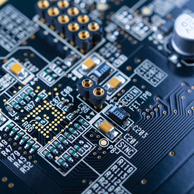
PCB Design & Layout Services
From PCB design for embedded systems and IoT to complex environmental or electromechanical systems, Northwest Engineering Solutions can help you stay at the forefront of technological change.
IC Substrates & UHDI PCB Design
We offer cutting-edge capabilities for the IC substrate and ultra-high density interconnect (UHDI) PCB markets with innovative designs, as well as chip-on-board, system-in-package (SiP), and multi-chip modules.
Signal Integrity Consulting
Applying 3D electromagnetic simulation software and proven analysis in PCBs/substrates to solve challenging signal integrity problems in high-speed digital designs and RF designs.
EMC Consulting
When a PCB design has problems passing EMC testing, have our team give your design a second look. We can recommend layout, grounding, stackup, and circuit changes that make big impacts on EMC.
PCB Design Training
Improve your company's PCB design skills with comprehensive training in advanced design areas, including cutting-edge topics like ultra-fast digital interfaces and ultra-HDI PCB design.
Technical Content for Electronics Engineers
Deeply researched technical content from industry leaders helps drive traffic and growth for EDA software companies, component vendors, and electronics manufacturers.
PCB Design Software Support


![]()
![]()
Prototype and Scale
We work with our PCB manufacturing partners to help you balance lead time, capabilities, cost, and standards compliance. Our PCB fabrication and assembly partners hold one or more of these quality and compliance certifications:
ISO 9001
AS9100
ISO 13485
ITAR, JCP, and/or NADCAP
Our partner capabilities include quick-turn prototypes, high layer count/HDI, high frequency, and specialty designs like ceramics and metal-core.

Markets We Serve
Target Markets and Verticals
ECAD/EDA Software Companies
PCB Manufacturers/EMS Companies
Commercial Space, Avionics, and Defense Electronics
Semiconductor Equipment Manufacturers
Embedded AI Hardware Companies
Advanced Materials Companies
Aerospace and Defense Electronics
We're an agile small business concern with a track record of excellence.
High-reliability mmWave products
Rugged power systems
Backplanes and modular embedded systems
Test and sensing equipment
DUNS# 080996092, CAGE# 80W03, Primary NAICS: 54171
Learn more about our defense and aerospace solutions.

Commercial Space
Let us help you take your designs into the stratosphere.
Rugged HDI PCB design and production
Microwave communications systems
High efficiency power management and regulation systems
Low-noise mixed-signal sensing platforms

Data Center Electronics
Our hardware supports modern data center infrastructure and operations.
High speed PCBs operating at 56G+
Multi-gig networking equipment
Aggresive form factor products
Power management systems
Data center IoT platforms

Industrial Automation
We develop and manufacture processing and testing systems for major semiconductor manufacturers and EMS companies.
Rackmount industrial single-board computers
PCBAs supporting new high speed digital and RF chipsets
High-power processing and testing systems
Evaluation and development products for chipmakers

Military IoT and Edge Computing
We bring rugged computing, sensing, and data management capabilities to warfighters operating at the edge.
Custom ruggedized IoT platforms
Standard form factor products (OpenVPX)
Hardware supporting embedded AI applications
PCBAs supporting embedded vision and sensor fusion systems

Smart Logistics
Our smart asset tracking products give you real-time access to critical data on your most valuable shipments.
Embed devices with critical shipments
Track assets worldwide in real time
Integrated tamper-proofing features
Capture data with your existing web stack

Innovative Electronics Design Solutions
We integrate systems across domains and keep you at the cutting edge.We don't sell one-size-fits-all products or services, we provide solutions to your most difficult technological challenges. Our specialties span electronics, embedded computing, and IoT from simple devices to mission-critical systems.
Taking Your Designs to Production
We work with advanced PCB manufacturing partners to help you prototype and scale.Ready to make the transition to production? Our network of advanced manufacturers can help you produce QTY 1 or QTY 1 million. We help you manage vendor selection, the PCB design review process, sourcing and procurement, and compliance.
Turning Insights Into Action
Deeply researched technical content, written by engineers for engineers.Our insights are key to driving growth for our EDA software and manufacturing clients. We know how to communicate the value of your products because we've built them and we use them. Work with us to position your company as a technical leader in the electronics industry.
Our Clients and Partners


